Solid State Triodes
The Transistor
In this lab we'll be building a three-transistor germanium PNP audio amplifier. The circuit will run on 9V and consume a relatively small fraction of the power of our previous tube-based designs while delivering superior audio (about 2W as opposed to the 10W of our tube amp). The technological progress from the first six labs will be palpable.
The Setup
Towards the very end of 1947, engineers at Bell Labs developed the first functional transistor, and in the years following, the device was perfected and developed rapidly. While the majority of modern (2024) transistorized electronics function using the Field Effect (forming Field Effect Transistors aka FETs), early transistors were point contact before evolving into bipolar junction transistors (BJTs) which were the dominant version up until the 1970s. Furthermore, in the first decade of transistor development, germanium (not silicon) was the semiconductor of choice. Germanium, which we've already utilized as a detector in the earlier FM radio, is in the same column as silicon in the periodic table.
While both NPN and PNP type transistors were developed early, due to various fabrication challenges and difficulties, PNP-type were the transistor most widely available at least at first with germanium. This was particularlarly interesting to a field of engineers coming from vacuum tubes since:
- The devices could use very low voltages (often well below 10V) where previously, tubes would need 100's of V to run properly.
- The devices used very little power (mW) where previously, tubes would need Watts just to even work. This is because the generation of charge carriers was "built-in" to the transistor's material properties whereas tubes relied on thermionic emission (which could only be obtained via inefficient resistive heating).
- BJTs were current-controlled current-source devices, as opposed to tubes which are voltage-controlled current-source devices. This required different ways of designing and thinking about the circuits.
- PNP BJTs (the most-common type at first) relied on holes as the charge carriers rather than electrons. This mean that the electrical positioning of BJTs was backwards to tubes. The "source" of the charge carriers (emitter in BJTs and cathode in tubes) was at opposite voltages.
A PNP BJT worked by injecting a certain amount of current into the base-to-emitter. This current would then result in a much larger current flowing from the collector to the emitter. There would be an amplification factor h_{FE}, which was actually a calculated slope from the device's I-V characteristics that would relate state that i_{CE} = h_{FE}\cdot i_{BE}. This amplification factor could be in the double-digits or maybe even a hundred or so.
One down-side with BJTs compared to tubes was that since they used an input current at their base to amplify, they generally had a lower input impedance than tubes.
The Transistors
In the United States, Western Europe and Japan, commercially available transistors started showing up in the mid-1950's. Many of these models like the CK722 are quite hard to acquire today, and when you can get them, they'll be very expensive to the point that building with them is a costly endeavor. They just were not produced for that long because newer and better models came around very quickly and the transition to silicon happened by the mid 1960's in almost all areas. Couple that with the fact that transistors didn't fail at the rates of tubes and the early ones didn't stick around long-enough to get included in a lot of early commercial (i.e. large volume) equipment, and there just aren't the massive warehouses of 50's germanium transistors like you see with particulr tube models (like the 6J6, 6AQ5, 12CN5, etc that we used in previous labs). It is an interesting predicament to find oneself when wanting to work with them. The solution arrives from abroad...
At the same time of the rapid development of transistors in the West, on the other side of the so-called "Iron Curtain" existed a land where production quotas were almost completely decoupled from actual demand, and making massive stockpiles of parts was not just common, but institutionally encouraged. As a result, many styles of early transistor (or equivalents) were manufactured in huge numbers up until the early 1990's. With the collapse of the Soviet Union in 1991, these stockpiles started to get sold off (and still do to this day). As a result we can acquire and use these 1950's era transistor models quite easily and cheaply to build our circuits.
Soviet Transistors
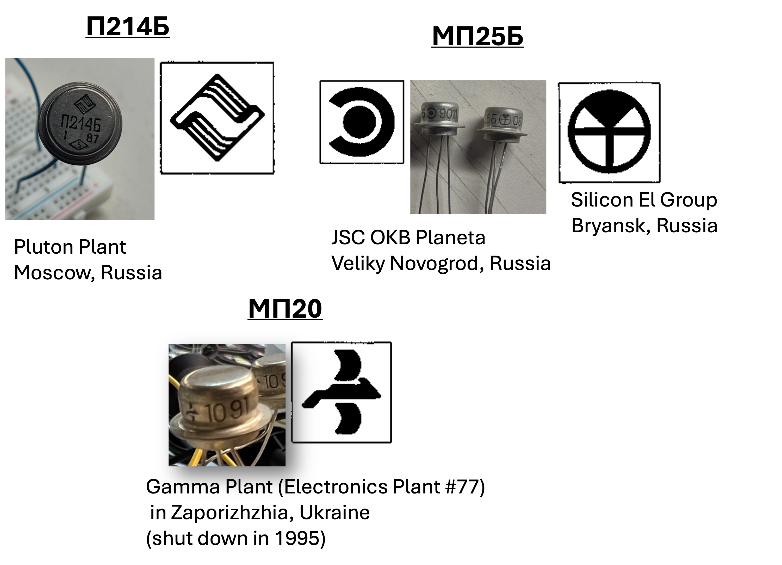
We'll be using three different Soviet-era germanium transistors:
- The MП25Б (or MP25B) PNP germanium transistor: This is a low-power decent generic transistor good as a pre-amp of sorts. It is capable of a current gain of <50 and output currents of maybe 10 mA.
- The MП20 (or MP20) PNP germanium transistor: This is a mid-power decent transistor. We'll use this as a power-amp driver. It is capable of current gains closer to 50, but an output current of 100 mA or more depending on biasing.
- The П214Б (or P214B) PNP germanium power transistor: This is a beefy power transistor meant for moving some serious current and power. Its current gain isn't amazing (maybe 40), but it can move a lot of current, provided you can feed it.
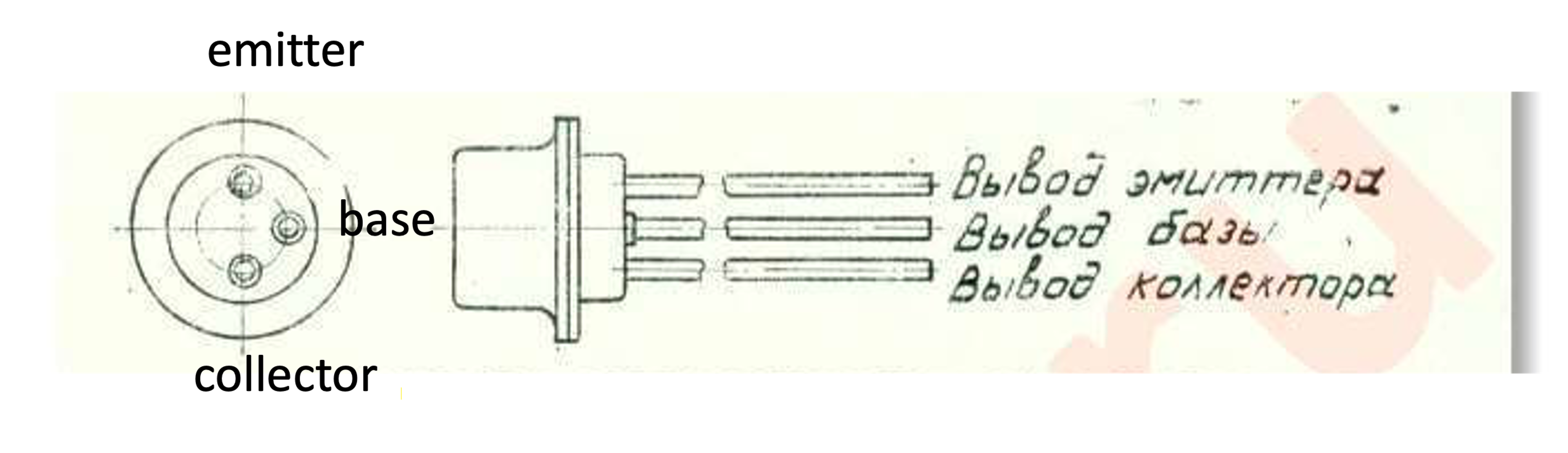
All three transistors come in a cool flying-saucer-like packaging. The MП25Б and MΠ20 transistors are smaller and have the following pinout:
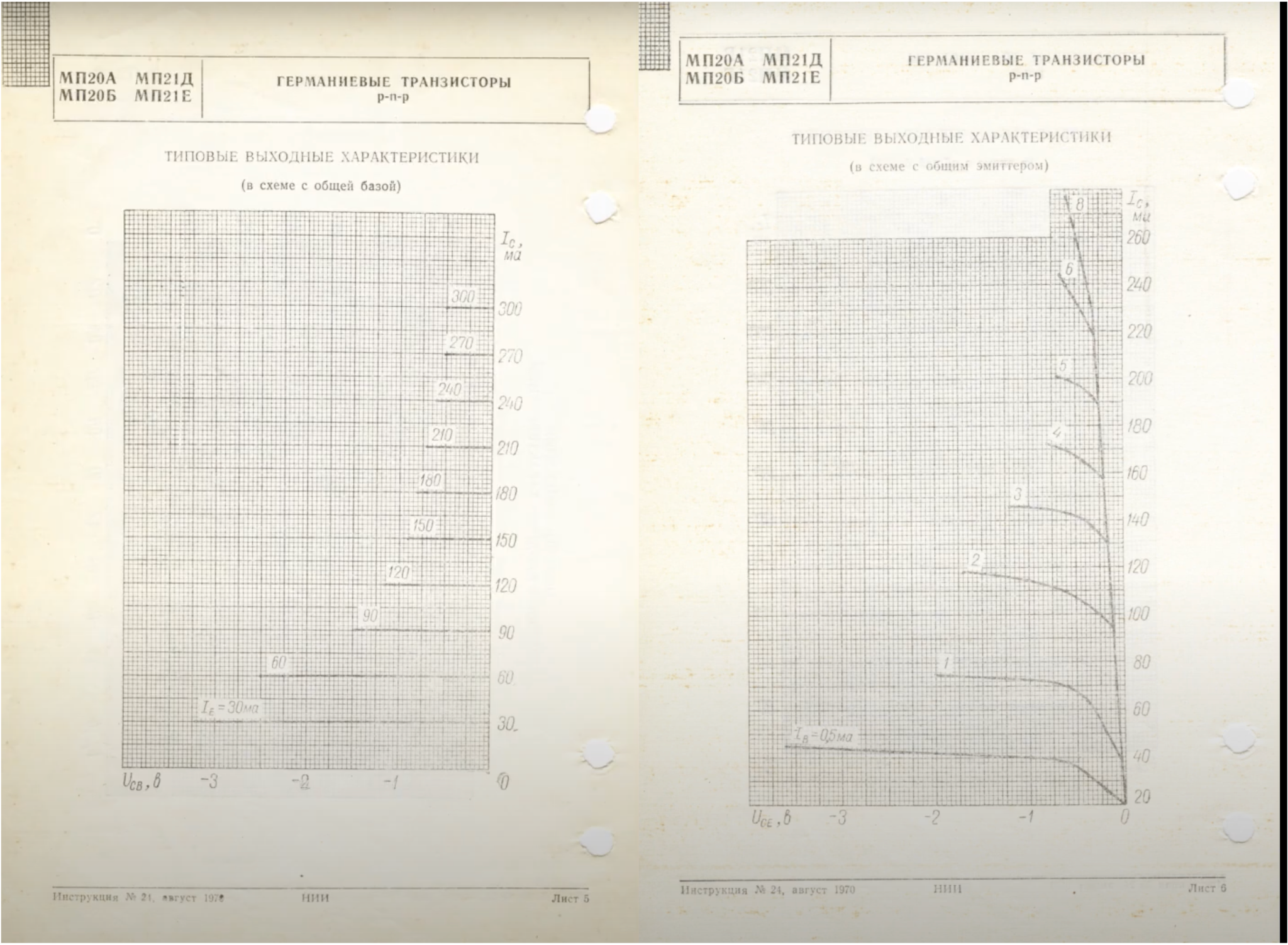
I can't find a MP25 datasheet but it is pretty generic to the point where we don't need to worry about it. The MP20 datasheet is out there, but it is hard to find I-V curves. Lukcly I found it on Youtube, of all places. Some channel is doing God's work putting these hard-to-find datasheets in a accessible location, but using the absolute worst means of disseminating the information (videos of pdfs...who does that?). Anyways, go to Open Electronic's youtube channel and smash that mf-ing like button.
Here's a screenshot from the relevant pages showing the I-V curves for the MP20. Notice they actually have two sets of curves...one from the BJT in saturation and cutoff modes and one in active mode. Interesting. Don't see that too much.
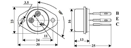
The P214B transistor is harder to find curves for. I did find its datasheet here (another Youtube channel archiving weird things). The pinout is here:
The transistors should be clearly marked with their numbers in Cyrillic. There will be a ton of other marks. The number is the date of manufacture. Most of the ones I have are from the late 1980s to early 1990s. There are symbols on all the transistors indicating what factory they were created in (I made a little key below). Some will have a rhombus as well which is a mark used to indicate that the transistor was "military-quality" which is very common to see since the Soviet Union had a rather small consumer electronics ecosystem up until its collapse.
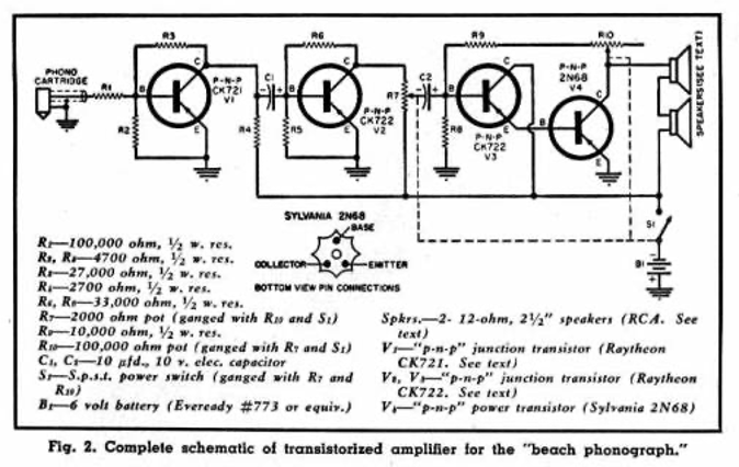
The Circuit
OK now to the circuit. It is a three-stage PNP-only Class-A amplifier audio amplifier. The three stages are:
- A common-emitter amplifier for voltage gain
- A emitter follower amplifier for current gain
- A second emitter follower amplifier for even more current gain and as a speaker driver.
The last two stages could be said to be one combined stage in the form of a PNP Darlington pair...that's a totally fine way to think about it too.
The term "Class A" for this amplifier refers to the fact that there is a significant amount of quiescent current running through the final output stage even when no signal is being transferred. The circuit is "on" at rest. Then the signal shows up as varying degrees of more-on and less-on around this rest point, if that makes sense. This is effectively what we did with our tube amp's last output stage as well in [COURSE/labs/lab04](Lab 04). This time, however, the quiescent current will be very large...like a quarter of an amp. From a modern design perspective, this is not great since we're using a ton of power when we're doing nothing, but believe it not, a lot of audiophiles like Class-A amplifiers since they don't have all the turn-on-turn-off behavior of other complementary output stages like
Without a output transformer (Which can take up a lot of space and cost and is), a Class A amplifier isn't a bad idea. Maximum efficiency will be somewhere around 12.5% with this system. Not great, but way better than our tube amp. Also when properly tuned, you should actually have some pretty decent output volume and you should have some bass this time around. I was listening to LCD Soundsystem earlier on my amp and while one may say a lot of things about LCD Soundsystem, let it not be said that they're a bass-light band.

Stage 0: Audio Input

Very similar to input stage in our tube amp. We merge the left and right audio stages using the resistors R_1 and R_2 and then feed the signal into the first stage through a DC-block cap C_1. The capacitor values aren't super strict here. 100 uF or 33 uF is probably fine. Larger values will give better bass response, however they will also take longer to "learn" on power up and stabilize the circuit.
Stage 1: Common Emitter Amplifier Preamp

This stage is very similar to the first two stages of the tube amplifier. It is a common-emitter amplifier. We don't need to bias it in a weird way with grid leak. Instead resistors R_3 and R_4 form a quasi-voltage divider which positions the base voltage at about mid-rail. The emitter voltage is therefore slightly above that (about 0.1V higher due to the junction drop of Germanium).
Gain of the circuit is based on the resistor R_6 but is tempered by resistor R_5, at least at DC. For signals (AC) we have capacitor C_2 which shorts out R_5 so that a large gain is applied to the signals. The output is tapped at the collector of the transistor.
Stage 2: Volume and First Buffer

The output of stage 1 is fed into a potentiometer being used as a variable voltage divider. This effectively acts as a volume control. The output is taken at the tap of the pot and fed through a DC block cap to isolate the different stages.
Transistor Q_2 is set up as an emitter-follower (which is functionally the same as the cathode-follower of our tube amp experience). Resistor R_8 will need tuning once the whole amp is built to try to position the output of the final stage at the middle of its range (4.5V) and to try to minimize Quiescent current. Note an optional pullup resistor (marked as R_{8B} might be useful to add in if you find that your system isn't behaving super well).
Stage 3: Second Buffer and Speaker Driver

The final stage is a second, beefier buffer circuit, taking the voltage that was handed into Q_2 which then buffered it into Q_3 which then buffers it into the demanding low-impedance load. Resistor R_9 MUST MUST MUST be a 5W "sandblock" power resistor (they are white and I have them at the front). This resistor is the DC bias load and will bleed off a lot of power. It will get warm. A little 1/4W resistor will smoke itself out if used so do not.
When signals come through, instead of going through the resistor, they will bridge through the big juicy C_4 capacitor linking in the speaker so that it gets a decent amount of signal and makes the noise we so desperately desire.
Note we are capacitively coupling to our speaker here (wherease before we coupled through a transformer). This is indicative of just how nicely our transistors can work with load-impedance loads like speakers compared to our tubes of the other week which have significant output impedance meaning we need more impedance matching (the transformer, for exmaple).
Testing
At power-up I got a quiescent current of about 0.3A at 9V. If you're getting significantly more, then you should power down and figure out what is up. Once your current is about right, then adjust the potentiometer R_8 while playing a signal to get best performance. You may want to add a ~22K resistor as a pullup from the base of Q_2 to stabilize the two final stages, though in my experience that wasn't 100% necessary and is somewhat dependent on what transistor you get.
Volume and sound quality of this sysystem should be pretty good...it should actually be enough that someone might tell you to "turn it down." :)